


232 Gongneung-ro, Nowon-gu, Seoul, 01811, korea
Tel : +82-2-970-6114,7114 Fax : +82-2-970-6088
Tel : +82-2-970-6114,7114 Fax : +82-2-970-6088


| Title | Professor Ok Jong Geol’s Research Team Develops a Tailored-Smart Nanopatterning Technology by Continuous Nanoinscribing | ||||
|---|---|---|---|---|---|
| Writer | admin | ReadCount | 2618 | Date | 2019-11-26 |
| Files |
|
||||
|
Professor Ok Jong Geol’s Research Team Develops a Tailored-Smart Nanopatterning Technology by Continuous Nanoinscribing
Dr. Ok’s team was able to provide an alternative to current high-cost vacuum processing and chemical etching processes. This advancement marks a breakthrough in the nanopatterning field.
Professor Ok Jong Geol and his team of Automotive Engineering Program in the Department of Mechanical and Automotive Engineering at SeoulTech presented the results of the research on “Tailored Nanopatterning by Controlled Continuous Nanoinscribing with Tunable Shape, Depth, and Dimension.”
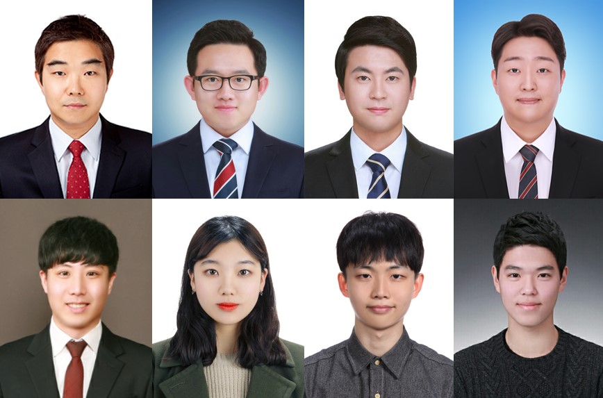
▲ Photo of participating research staff. In the first row from left to right: Professor Ok Jong Geol, Oh Dong Gyo, Lee Seung Jo (Graduate researchers), Lee Won Sik. In the second row from left to right: Yeon Gyu Beom, Lee Na Young, Jung Soon Min, Kim Dong Ha (Undergraduate researchers).
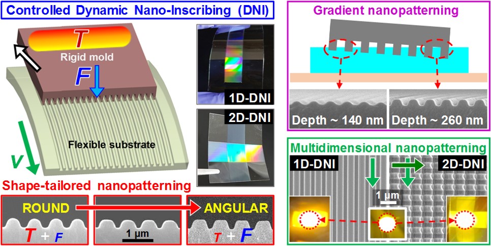
Nanopatterns are key components that are being applied in fields such as mining, communications, sensors, biotechnology, and energy, as well as indisplays and semiconductors, due to its unique of microscopic structure and optical characteristics, such as large surface area, mutual interference with light, etc.. Nanopatterns are currently manufactured through photolithography and laser interference processing methods, but they require complex and costly equipment, materials, and processes. In order to solve these problems, dynamic nanoinscribing, or DNI, was announced as a concept in the US in 2009. However, due to complications involving the mechanism, the effects of processing factors, and tailored control and applications, further research was needed.
▲ Example of tailored nanopatterns manufactured through nanoinscribing and mimetic diagram of the nanoinscribing process
Nanoinscribing technology is different from pre-existing face-to-face methods that use vacuum and etching processes to drill wafers on wafers. Instead, nanoinscribing technology uses only top-of-the-line pattern molds to inscribe (line-to-face), which is considered to be a state-of-the-art processing technology that allows for high-speed and low-cost continuous nanopatterning over large surfaces.
Professor Ok’s team created a nanoinscribing system that is both simple and precise. The team classified the factors affecting the manufacturing of nanopatterns by processing strength, temperature, and speed as they researched systemic factors. They were also able to define the correlation between the factors and the final nanopattern formations and presented a theoretical model that supported their analysis. Furthermore, these different tailored nanopattern results based on nanoinscribing provided many practical optical element applications, which is also expected to be an area of future research.
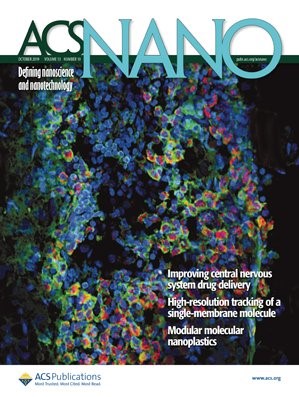
▲ Cover of ACS Nano journal that published the research results
The results of the research were lauded for their creativity and practicality and were published in the October edition of the ACS Nano (Nanoengineering JCR Top 6% (IF 13.903). (http://doi.org/10.1021/acsnano.9b04221)
The research was supported by the Ministry of Science, the Technology and Information Communications Leading Research Center Support Project, and the Ministry of Education’s Engineering University-Focused Research Institute Support Project. SeoulTech Professor Lee Sang Hoon, Hanyang University Professor Park Hee Joon, Aju University Graduate Researcher Lee Seung Hoo, and Samsung Display Lead Researcher Han Gang Soo participated in the research along with Professor Ok’s team.
|
|||||

SeoulTech Signs MOI for City Planning with the Government of El Salvador

SeoulTech Hosts the 2019 SeoulTech Intelligent Robots Competition
